
Carat Systems develops nanocrystalline and ultra-nanocrystalline diamond coatings on selected substrates when the application requires diamond surface chemistry, dielectric behavior, wear resistance, plasma compatibility, erosion resistance, or a controlled nucleation layer for later diamond growth.
The film structure is selected for the application. Nanocrystalline diamond (NCD) can provide thicker, more textured diamond coatings, while Ultra-Nanocrystalline Diamond (UNCD) provides a much finer-grained surface morphology for thin-film coating applications.
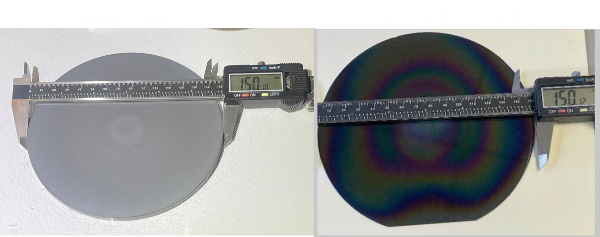
150 mm diameter wafer coated with nanocrystalline diamond, NCD, on the left, and 150 mm diameter wafer coated with Ultra-Nanocrystalline Diamond, UNCD, on the right.
Ultra-Nanocrystalline Diamond, or UNCD, is a fine-grained CVD diamond film used where conventional microcrystalline diamond is too rough, too thick, or not well matched to the substrate. UNCD can provide diamond-like chemical resistance, dielectric behavior, wear resistance, and surface coverage while maintaining a much finer surface morphology than larger-grain diamond films.
Carat Systems uses UNCD and related nucleation routes as part of diamond coating and process development work. The correct film structure depends on substrate material, target thickness, adhesion requirement, surface finish, thermal environment, and whether the coating is being used for wear, plasma compatibility, dielectric isolation, optical behavior, or later diamond growth.
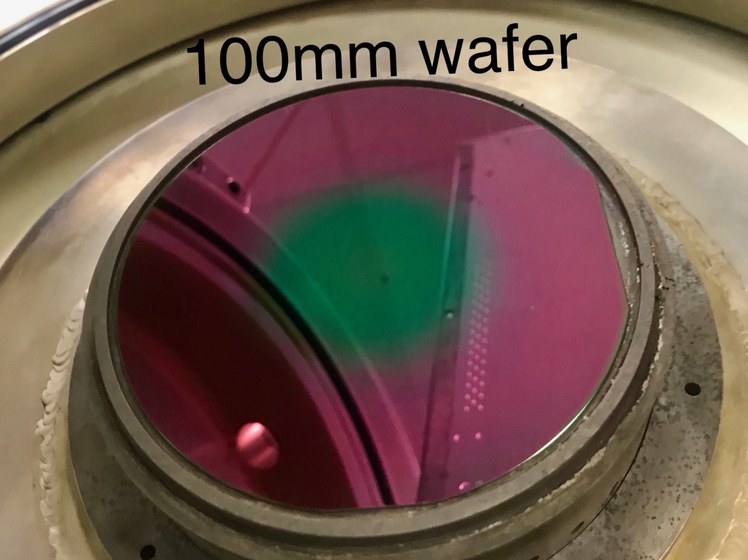
Ultra-Nanocrystalline Diamond coated silicon wafer example.
CVD diamond is not one product. The right material depends on crystal form, nucleation route, grain structure, thickness, polishing, thermal path, dielectric requirement, and the customer's operating environment.
Many technical diamond programs fail because the material specification is separated from the growth process. Thickness, stress, bow, roughness, grain structure, nucleation, polishing, thermal contact, and substrate compatibility are coupled. Carat can help define the process route before a customer commits to production hardware or a narrow material specification.
For a useful first review, send the substrate or part geometry, target thickness, surface finish requirement, application temperature, environment, electrical or optical constraints, and whether the desired path is sample material, process development, or reactor purchase.
These categories should be treated as starting points for a technical discussion. Final feasibility depends on geometry, substrate, required thickness, polishing, stress tolerance, and metrology requirements.
Diamond-on-silicon and diamond plate development for heat spreading, high power density devices, and advanced electronics packaging.
Diamond plates and windows for applications needing transparency, dielectric strength, plasma compatibility, chemical resistance, or high thermal conductivity.
Polycrystalline diamond material has demonstrated charge collection behavior relevant to particle and radiation detector applications.
Ultra-nanocrystalline diamond coatings for thin-film applications where nucleation, surface morphology, and substrate compatibility matter.
Diamond material and process development for NV center and quantum research programs, with requirements reviewed case by case.
Process development for unusual substrates, special geometries, nonstandard thickness targets, and application-driven material specifications.
Representative examples below show CVD diamond growth capability across special geometries, ultra-nanocrystalline coatings, and wafer-scale process development.
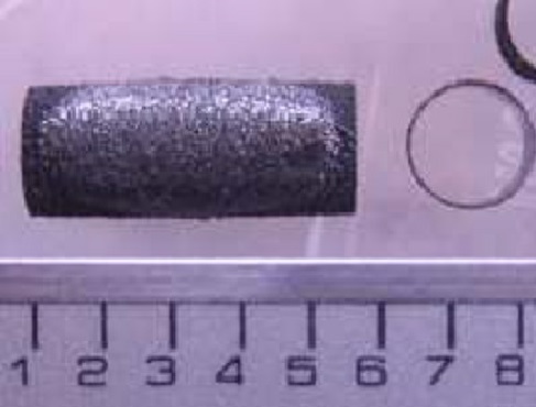
Solid diamond tube waveguide for Ka-band work and special geometry CVD diamond applications.
Ultra-nanocrystalline diamond coated silicon wafer example.
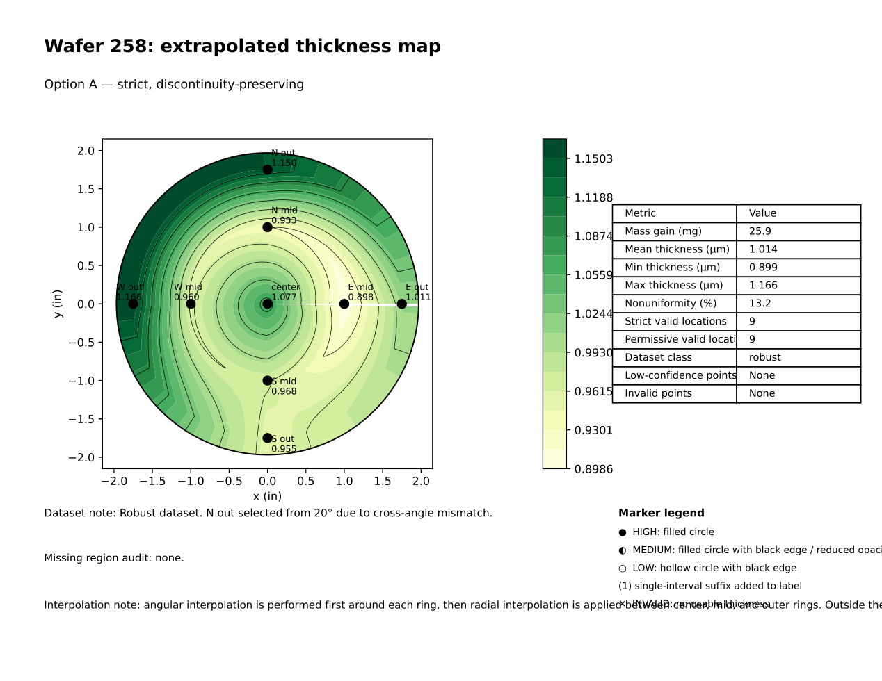
Thickness mapping and process feedback for CVD diamond wafer development. View process development and metrology.
For single crystal diamond, gem growth, or personal CVD diamond inquiries, use the links below.
View single crystal gem examples or send a custom gem inquiry.