
Free-standing CVD diamond can be supplied or developed in polished and unpolished forms depending on the optical, thermal, detector, or research requirement.
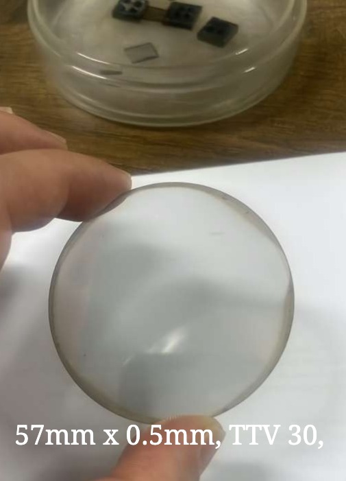
Polished free-standing optical CVD diamond wafer example, approximately 57 mm diameter and 0.5 mm thick.
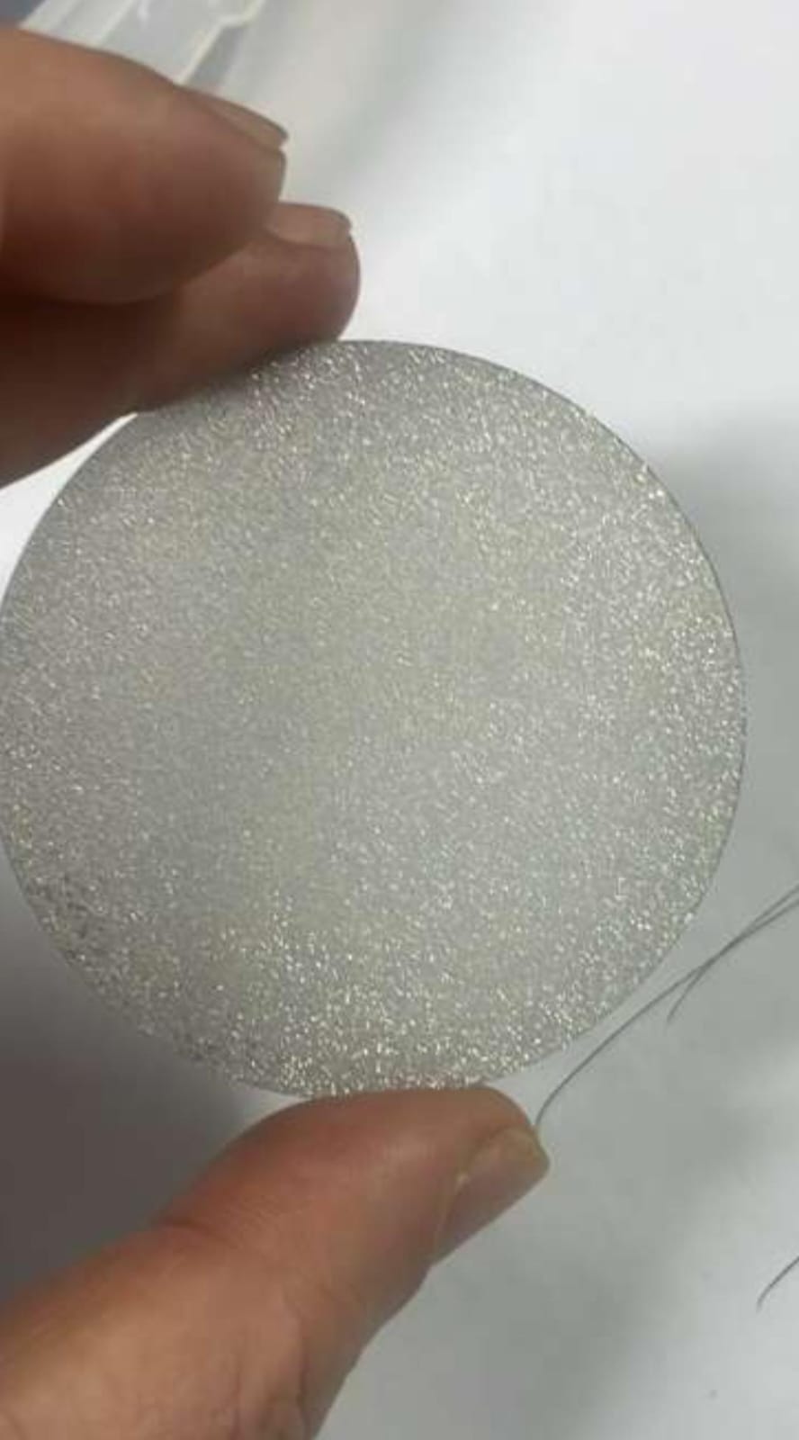
Unpolished free-standing optical CVD diamond wafer example before final surface polishing.
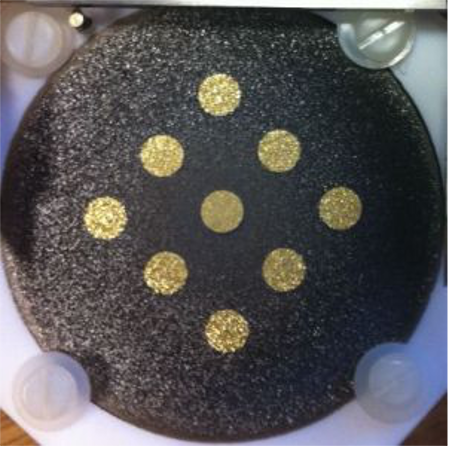
Metallized thermal diamond wafer example used to evaluate electrical, detector, or thermal-interface behavior.
Representative Raman spectroscopy at 532 nm on a 115 micron thick diamond layer shows a strong diamond peak centered near 1332 cm-1 with no graphitic shoulder. Across seven points along the 100 mm wafer diameter, the reported average FWHM was 3.8 cm-1 with a 0.8 cm-1 standard deviation.
This supports the central technical claim: Carat's high-power MWCVD platform can produce high quality, wafer-scale CVD diamond films suitable for thermal, photonic, detector, and advanced device development.
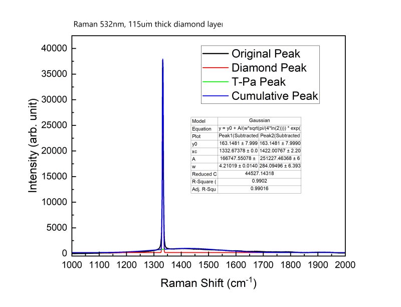
Representative Raman spectrum at 532 nm for a 115 micron thick CVD diamond layer. The diamond peak is centered near 1332 cm-1.
CVD diamond wafer and plate projects require more than a nominal thickness target. Thickness distribution, edge behavior, mass gain, and measurement confidence determine whether a material result is ready for the next development step or needs process adjustment.
The example at right shows a 100 mm class wafer thickness map generated from nine measurement locations using a strict, discontinuity-preserving interpolation method. The analysis reported a 25.9 mg mass gain, 1.014 µm mean thickness, 0.899 µm minimum thickness, 1.166 µm maximum thickness, and 13.2% nonuniformity for a robust dataset with no invalid locations.
This type of mapping helps identify radial and azimuthal growth trends, compare process conditions, and decide whether the next development step should focus on plasma coupling, substrate temperature, gas chemistry, nucleation, or fixture geometry.
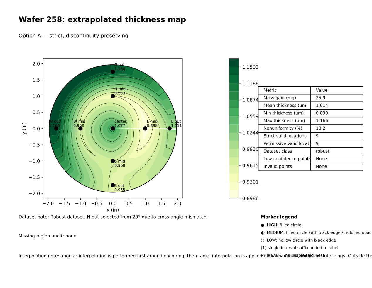
Representative CVD diamond wafer thickness map and analysis table. Wafer 258: mean thickness 1.014 µm, min 0.899 µm, max 1.166 µm, nonuniformity 13.2%, robust dataset.
Send substrate dimensions, target diamond thickness, required surface finish, application environment, and any acceptance criteria. Carat can help determine whether the proper next step is a sample coating, process development program, material supply discussion, or reactor configuration review.