Carat Systems logo
Microwave plasma CVD diamond technology

Microwave Plasma CVD Diamond Platforms for Thermal, Semiconductor, Quantum, Optical, and Fusion Applications

Carat Systems develops microwave plasma CVD diamond platforms and process windows for applications where diamond performance is limited by scale, interface quality, nucleation control, thermal stress, or process reproducibility.

Carat helps turn CVD diamond from a lab material into an application-specific manufacturing process by connecting reactor design, plasma behavior, substrate-specific nucleation, thermal control, and metrology-driven development.

Polished CVD diamond wafer developed by Carat Systems

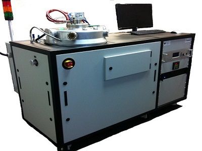
CTS10U microwave plasma CVD diamond system for wafer coating, single-crystal growth, bias-enhanced nucleation, in-situ thickness metrology, and process optimization for technical applications.

What Carat Systems provides

Carat combines reactor hardware, diamond growth process knowledge, BEN-enabled nucleation, large-area microwave plasma scaling, and process metrology development. This lets customers connect material requirements to a manufacturable process path instead of treating the reactor, film, substrate, and metrology as separate problems.

Microwave plasma CVD reactors

Research and pilot production diamond CVD systems for electronic diamond, optical diamond, thermal management, and gem growth programs.

  • 2.45 GHz MPCVD systems up to 15 kW
  • 915 MHz MPCVD systems up to 115 kW
  • High-purity process design
  • Custom reactor configuration
  • Control software and upgrades

View CVD systems

CVD diamond materials

Polycrystalline diamond wafers, plates, coatings, and diamond-on-silicon development for thermal, optical, electronic, and research applications.

  • Diamond-on-silicon wafers
  • CVD diamond plates and windows
  • Thermal spreader development
  • Custom substrate coating

View CVD diamond wafers and plates

Process development and metrology

Diamond process development for film uniformity, bow, Raman quality, nucleation, polishing, and scale-up to customer applications.

  • UNCD and BEN capability
  • Thickness mapping and reflectometry
  • IR thermal mapping development
  • Technology transfer and training

View process development and metrology

Where Carat fits in emerging CVD diamond opportunities

CVD diamond is moving from a specialty material toward application-specific manufacturing in thermal management, semiconductor packaging, quantum materials, optics, and fusion. The limiting problems are often not only diamond growth, but scale-up, interface quality, nucleation, stress, uniformity, substrate coupling, and process control.

Carat works at that intersection: microwave plasma reactor design, diamond growth process windows, substrate-specific nucleation, thermal behavior, and metrology-driven development.

Scale

Large-area microwave plasma CVD development for programs moving from 100 mm toward 150 mm, 200 mm, and 300 mm class diamond growth.

  • 2.45 GHz and 915 MHz process perspective
  • Power, pressure, plasma footprint, and thermal design tradeoffs
  • Prototype design versus production optimization

Interface

Diamond-on-silicon and diamond-on-semiconductor process development where adhesion, stress, thermal contact, and substrate compatibility matter.

  • Thermal spreader and semiconductor packaging applications
  • Substrate-specific growth and stress management
  • Transition from sample coating to equipment path

Nucleation and control

BEN, UNCD, reflectometry, thermal mapping, and Raman-oriented process feedback for cleaner and more reproducible diamond growth.

  • Bias-enhanced nucleation and UNCD routes
  • Thickness and temperature mapping development
  • Metrology-driven process optimization

Applications

Carat works with customers where CVD diamond properties matter: thermal conductivity, optical transparency, chemical resistance, plasma compatibility, radiation hardness, and high electric-field performance.

Carat is most relevant where the customer needs a diamond process, not just a diamond part: substrate preparation, nucleation, growth, stress control, uniformity, metrology, and eventual transfer to equipment or production.

Semiconductor thermal management
Diamond-on-silicon thermal spreaders
Fusion target coatings
Optical diamond windows
UNCD coatings
BEN nucleation on silicon
High-power electronics
Quantum and research materials

Development capability beyond equipment sales

Carat helps turn CVD diamond from a lab material into an application-specific manufacturing process. For demanding programs, the value is not only the reactor. It is the coupled reactor, plasma, substrate, nucleation, thermal, stress, and metrology problem.

  • Thin and thick diamond film process development
  • Thickness uniformity and bow optimization on 100 mm substrates
  • Diamond-on-silicon routes for thermal spreader applications
  • Sample coating programs and transition to equipment or production paths
  • Design-basis reviews for CVD diamond scale-up, including substrate size, power and pressure envelope, thermal management, uniformity risk, diagnostics, and process-transfer path

View process development and metrology

Start with a technical review

Send the application, substrate material, substrate size, target thickness, required uniformity, quality metrics, temperature limits, contamination constraints, and metrology needs. We can help determine whether the next step should be a design-basis review, sample coating, process development program, or reactor discussion.

Send specifications

Selected electronic diamond and technical customers

Have a CVD diamond process, material, or equipment requirement?